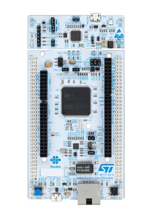
NUCLEO-F767ZI: Difference between revisions
Jump to navigation
Jump to search
No edit summary |
|||
| Line 16: | Line 16: | ||
* I2C (4) | * I2C (4) | ||
* SPI (6) | * SPI (6) | ||
* QSPI (2) Bank1 and Bank2 (Up to 216 MHz) | |||
* General Purpose Timers (10) | * General Purpose Timers (10) | ||
* Advanced-control Timers (2) | * Advanced-control Timers (2) | ||
Latest revision as of 11:41, 30 May 2023
The NUCLEO-F767ZI development board uses the STM32F767ZI as the target processor.
This board is a rock solid development board with on-board ST-Link loader / debugger, using an STM32F103CBT6.

STM32F767ZIT6 in LQFP144 package
- ARM®32-bit Cortex®-M7 + DPFPU + Chrom-ART™ Accelerator
- 216 MHz max CPU frequency
- VDD from 1.7 V to 3.6 V
- 2 MB Flash
- 512 KB SRAM
- GPIOs (114) with external interrupt capability
- 12-bit ADCs with 24 channels (3)
- 12-bit DAC channels (2)
- USART/UART (8)
- I2C (4)
- SPI (6)
- QSPI (2) Bank1 and Bank2 (Up to 216 MHz)
- General Purpose Timers (10)
- Advanced-control Timers (2)
- Basic Timers (2)
- Low-power Timers (1)
- Watchdog Timers (2)
- CAN 2.0B active (3)
- SAI (2)
- SPDIFRX 4 inputs
- SDMMC
- Camera Interface
- LCD-TFT Interface
- USB 2.0 OTG HS/FS
- Random Number Generator (TRNG for HW entropy)
- Ethernet
NUCLEO-767ZI Board Hardware
Power indicator, green LED, LD6, illuminates when power is applied
Green LED, LD1, connected to PB0, illuminates when driven high
Blue LED, LD2, connected to PB7, illuminates when driven high
Red LED, LD3, connected to PB14, illuminates when driven high
Bicolor Red/Green LED, LD4, illuminates during ST-Link activity
Green LED, LD8, illuminates when power is enabled/applied to target USB VBUS
Blue PushButton, B1, connects to PC13, creates a high signal (VDD) when pressed
32,768Hz crystal oscillator, LSE, used for Real Time Clock (RTC), connects to PC14 & PC15
8MHz HSE, is provided by the 8MHz crystal oscillator from the attached ST-Link, into PH0
UART3 connects the target processor to the ST-Link, providing a USB COM port connection on the host computer. Uses PD8 for TX, and PD9 for RX.
ST-Link connects to TCK (PA14), TMS (PA13)
10/100 Ethernet Connections
RMII_TX_EN, PG11
RMII_TXD0, PG13
RMII_TXD1, PB13
RMII_RXD0, PC4
RMII_RXD1, PC5
RMII_CRS_DV, PA7
RMII_MDC, PC1
RMII_MDIO, PA2
RMII_REF_CLK, PA1
Where is everything?
Once an STM32 processor or development board is selected, STM32CubeIDE downloads and installs
a firmware package for the device selected.
I found the install location for the “F1” firmware here:
C:\Users\JimMerkle\STM32Cube\Repository\STM32Cube_FW_F7_V1.16.2
Within this folder are header files, HAL source code, middleware, driver code,
example code, and documentation for the firmware package.

Each project includes a copy of the header files needed for a build.
(Just drill down inside the project's Driver folder.)  Example:
C:\Users\JimMerkle\Documents\STM32_Projects\NUCLEO-F767ZI_Blinky\Drivers\STM32F7xx_HAL_Driver\Inc\stm32f7xx_hal_gpio.h
References
https://www.st.com/en/evaluation-tools/nucleo-f767zi.html
https://os.mbed.com/platforms/ST-Nucleo-F767ZI/