LittleFS Flash File System: Difference between revisions
No edit summary |
|||
| Line 1: | Line 1: | ||
= | =LittleFS Flash File System= | ||
I recently learned about a compact embedded Flash File System known as SpiFFS.<br> | I recently learned about a compact embedded Flash File System known as SpiFFS.<br> | ||
While researching SpiFFS, I soon learned of another compact embedded Flash File System, '''LittleFS'''.<br> | While researching SpiFFS, I soon learned of another compact embedded Flash File System, '''LittleFS'''.<br> | ||
| Line 9: | Line 9: | ||
* Maintains revision count and CRC (security features) | * Maintains revision count and CRC (security features) | ||
Let's put this file system onto | ==The Hardware== | ||
Let's put this file system onto an STM32 board and check it out. | |||
I'll be using a NUCLEO-F103RB ($10.34), with a Winbond W25Q128FVSG SPI Flash module from Ebay. | |||
If the link doesn't work, just search Ebay for "W25Q128 Module". I bought two for $8.26 (free shipping). | https://www.ebay.com/itm/264290947181 If the link doesn't work, just search Ebay for "W25Q128 Module". | ||
I bought two for $8.26 (free shipping). Download the PDF for the W25Q128FVSG: | |||
https://www.winbond.com/resource-files/w25q128fv%20rev.m%2005132016%20kms.pdf | https://www.winbond.com/resource-files/w25q128fv%20rev.m%2005132016%20kms.pdf | ||
| Line 28: | Line 28: | ||
So, we will use SPI2 bus and its signal pins.<br> | So, we will use SPI2 bus and its signal pins.<br> | ||
To connect up the signals for power and the SPI BUS, here's the wiring diagram that was used:<br> | To connect up the signals for power and the SPI BUS, here's the wiring diagram that was used:<br> | ||
'''Winbond W25Q128FVSG SPI Flash Module wiring:''' | |||
'''Signal Windbond Pin W25QXX Pin NUCLEO-F103RB Pin''' | '''Signal Windbond Pin W25QXX Pin NUCLEO-F103RB Signal & Pin''' | ||
DI 5 1 PB15 SPI2_MOSI CN10-26 | DI 5 1 PB15 SPI2_MOSI CN10-26 | ||
CLK 6 2 PB13 SPI2_SCK CN10-30 | CLK 6 2 PB13 SPI2_SCK CN10-30 | ||
| Line 36: | Line 36: | ||
CS 1 5 PB12 SPI2_NSS CN10-16 | CS 1 5 PB12 SPI2_NSS CN10-16 | ||
VCC 8 6 +3V3 CN7-16 | VCC 8 6 +3V3 CN7-16 | ||
==The Software== | |||
===The SPI and Serial Interface=== | |||
Let's start by getting enough in place to read the Manufacturer and Device ID from the Winbond part. | |||
Within the STM32CubeMX package for your project: | |||
* Enable SPI2 as "Full-Duplex Master"., | |||
* Hardware NSS Signal: "Disable" - We will use GPIO control for this signal. | |||
- Don't bother trying to use some form of SPI hardware control for this signal pin. | |||
* Frame Format - Motorola, 8-Bits, MSB First | |||
* Clock Prescaler 256, (140,625KBits/s - this can be changed later) | |||
* Clock Polarity - CPOL: Low (signal is normally low) | |||
* Clock Phase - CPHA: 1 Edge (first rising edge) | |||
* CRC Calculation: Disabled | |||
* NSS Signal Type: Software (GPIO contol) | |||
* Select PB12 Pin, change signal to GPIO_Output, name it "SPI2_NCS" (so we will be using the same names) | |||
* Configure the HCLK for 72MHz (this is rather optional). | |||
(The Winbond part will function well beyond what this STM32 processor can clock over the SPI bus) | |||
'''Optional configuration and code that will ease debugging''' | |||
Select and configure USART2 (The USART2 signals are routed to the NEUCLEO's ST-LINK chip, | |||
creating a serial connection to your host computer over USB.) | |||
* Mode: Asychronous, Hardware Flow Control (RS232): Disable | |||
* Baud Rate: 115200, 8 bits, No Parity, 1 Stop Bit, Data Direction: Receive and Transmit | |||
I Cloned '''littleFS''' to my local machine. | |||
Reference Information:<br> | Reference Information:<br> | ||
Revision as of 16:58, 10 October 2020
LittleFS Flash File System
I recently learned about a compact embedded Flash File System known as SpiFFS.
While researching SpiFFS, I soon learned of another compact embedded Flash File System, LittleFS.
LittleFS appears to be even more compact and has additional security in that it creates and maintains a CRC for each file, and verifies the CRC each time the file is read.
- Compact
- Power-loss resilience
- Dynamic wear leveling
- Bounded RAM/ROM
- Maintains revision count and CRC (security features)
The Hardware
Let's put this file system onto an STM32 board and check it out.
I'll be using a NUCLEO-F103RB ($10.34), with a Winbond W25Q128FVSG SPI Flash module from Ebay.
https://www.ebay.com/itm/264290947181  If the link doesn't work, just search Ebay for "W25Q128 Module".
I bought two for $8.26 (free shipping).  Download the PDF for the W25Q128FVSG:
https://www.winbond.com/resource-files/w25q128fv%20rev.m%2005132016%20kms.pdf
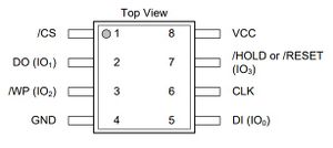
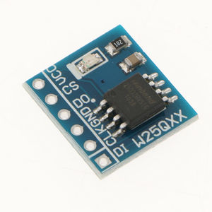
The W25Q128FVSG uses 2.7V to 3.6V for operation. Here's a diagram for the the chip's pins and signals,
along with the Ebay "W25QXX" module" photo:
 ]
] ]
]
Since the NUCLEO-F103RB powers its STM32F103RB processor with 3.3V, this "W25QXX" module"
is compatible with the NUCLEO-F103RB.  (The STM32-F103RB is capable of running from 2.0V to 3.6V.)
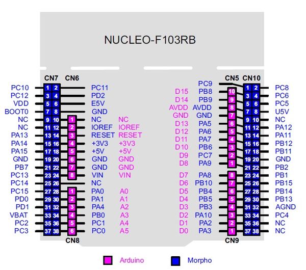
Let's look at the signal pins on the NUCLEO-F103RB:
 ]
]
On the NUCLEO board, the SPI1_SCK signal is being used to drive the board's Green LED.
So, we will use SPI2 bus and its signal pins.
To connect up the signals for power and the SPI BUS, here's the wiring diagram that was used:
Winbond W25Q128FVSG SPI Flash Module wiring:
Signal     Windbond Pin   W25QXX Pin  NUCLEO-F103RB Signal & Pin
  DI           5              1       PB15 SPI2_MOSI  CN10-26
  CLK          6              2       PB13 SPI2_SCK   CN10-30
  GND          4              3       GND             CN10-20
  DO           2              4       PB14 SPI2_MISO  CN10-28
  CS           1              5       PB12 SPI2_NSS   CN10-16
  VCC          8              6       +3V3             CN7-16
The Software
The SPI and Serial Interface
Let's start by getting enough in place to read the Manufacturer and Device ID from the Winbond part.
Within the STM32CubeMX package for your project:
* Enable SPI2 as "Full-Duplex Master".,
* Hardware NSS Signal: "Disable"  - We will use GPIO control for this signal.
  - Don't bother trying to use some form of SPI hardware control for this signal pin.
* Frame Format - Motorola, 8-Bits, MSB First
* Clock Prescaler 256,  (140,625KBits/s - this can be changed later)
* Clock Polarity - CPOL: Low (signal is normally low)
* Clock Phase - CPHA: 1 Edge (first rising edge)
* CRC Calculation: Disabled
* NSS Signal Type: Software (GPIO contol)
* Select PB12 Pin, change signal to GPIO_Output, name it "SPI2_NCS" (so we will be using the same names)
* Configure the HCLK for 72MHz (this is rather optional).
    (The Winbond part will function well beyond what this STM32 processor can clock over the SPI bus)
Optional configuration and code that will ease debugging
Select and configure USART2 (The USART2 signals are routed to the NEUCLEO's ST-LINK chip,
    creating a serial connection to your host computer over USB.)
* Mode: Asychronous, Hardware Flow Control (RS232): Disable
* Baud Rate: 115200, 8 bits, No Parity, 1 Stop Bit, Data Direction: Receive and Transmit
I Cloned littleFS to my local machine.
Reference Information:
https://uimeter.com/2018-04-12-Try-LittleFS-on-STM32-and-SPI-Flash/
https://github.com/ARMmbed/littlefs
https://github.com/ARMmbed/littlefs/blob/master/README.md