SSD1306 128x64 SPI OLED Display: Difference between revisions
Jump to navigation
Jump to search
No edit summary |
No edit summary |
||
| Line 20: | Line 20: | ||
RES# This pin is reset signal input. When the pin is pulled LOW, initialization of the chip is executed. | RES# This pin is reset signal input. When the pin is pulled LOW, initialization of the chip is executed. | ||
Keep this pin HIGH (i.e. connect to VDD) during normal operation. | Keep this pin HIGH (i.e. connect to VDD) during normal operation. | ||
D/C# This is Data/Command control pin. When it | D/C# This is Data/Command control pin. When LOW, it indicates a command to be sent to the command register. | ||
When HIGH, it indicates data. | |||
In I2C mode, this pin acts as SA0 for slave address selection. | In I2C mode, this pin acts as SA0 for slave address selection. | ||
When 3-wire serial interface is selected, this pin must be connected to VSS. | When 3-wire serial interface is selected, this pin must be tied low (connected to VSS). | ||
CS# This pin is the chip select input. (active LOW). | CS# This pin is the chip select input. (active LOW). | ||
Revision as of 20:57, 30 December 2020
Hardware


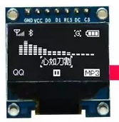
These displays use the SSD1306 controller: https://cdn-shop.adafruit.com/datasheets/SSD1306.pdf
The following is from the SSD1306.pfd document:
8.1.3 MCU Serial Interface (4-wire SPI)
The 4-wire serial interface consists of serial clock: SCLK, serial data: SDIN (MOSI), D/C#, CS#.
In 4-wire SPI mode, D0 is used for SCLK signal, D1 is used for MOSI. For the unused data pins, D2 should be left open.
The pins from D3 to D7, E and R/W# (WR#)# can be connected to an external ground.

Table 8-4 : Control pins of 4-wire Serial interface
Function	E(RD#)	R/W#(WR#)	CS#	D/C#	D0
Write command	Tie LOW	Tie LOW	L	L	↑
Write data	Tie LOW	Tie LOW	L	H	↑
Note
(1) H stands for HIGH signal
(2) L stands for LOW signal
RES#   This pin is reset signal input. When the pin is pulled LOW, initialization of the chip is executed.
       Keep this pin HIGH (i.e. connect to VDD) during normal operation.
D/C#   This is Data/Command control pin. When LOW, it indicates a command to be sent to the command register.
       When HIGH, it indicates data.
       In I2C mode, this pin acts as SA0 for slave address selection.
       When 3-wire serial interface is selected, this pin must be tied low (connected to VSS).
CS#  This pin is the chip select input. (active LOW).

NOTE: This device uses SPI mode 0.
For this exercise, I used the SPI (4 wire) Hardware interface, with reset (RES#) added. (I don't believe MISO is used.)
According to the datasheet, the maximum SPI clock frequency is 10MHz.
Connections
Board	       MOSI    MISO	SCK	RES#	CS#	D/C#
Arduino UNO	11	12	13	8	7	6
Software
For Arduino, the Adafruit SSD1306 library, version 2.4.2, works very well.
Additional Resources
https://learn.adafruit.com/monochrome-oled-breakouts/wiring-128x32-spi-oled-display